|
Package Internal
Structure

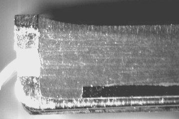
Cross Section of Student Package showing the Dual Inline Hybrid Package with
attached die and the cavity filled with encapsulant.
top

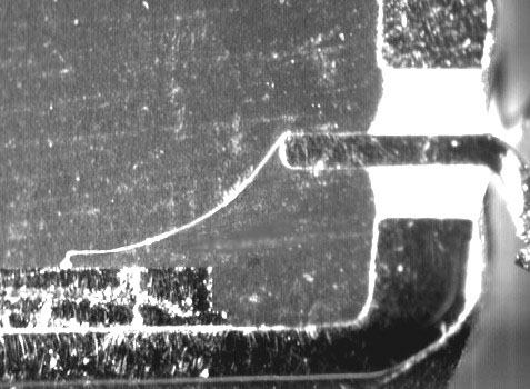
Close up cross section showing the wire bond from the die (ball bond at left
center) to the lead finger (wedge bond at center). The potting of the
lead to the package body is clearly evident in this view.
top

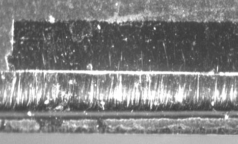
Die mounted to the Dual Inline Hybrid Package. The die attach adhesive
is evident in this view as the light colored line between the die and the
package.
top

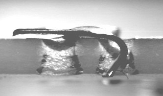
Section of lead soldered to the PCB. (The package body has been removed
from its earlier location on the bottom side of the PCB in this view.)
The roughly drilled holes in this inexpensive PCB are evident in this
view. The solder joint is in the top center of the picture. The
copper traces are on the top surface in this view.
|