|
Package Examples
PBGA (Plastic Ball Grid Array) (left)
and PLGA (Plastic Land Grid Array) (right)
The PBGA consists of the PLGA with the solder balls added. These are
Pentium II CPU's.
We will be dissecting the PLGA as part of Lab 1. (See Below)
top
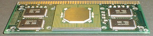
Pentium II CPU (PBGA from above) mounted onto its card.
top
TCP (Tape Carrier Package)
top
PPGA (Plastic Pin Grid Array)
top

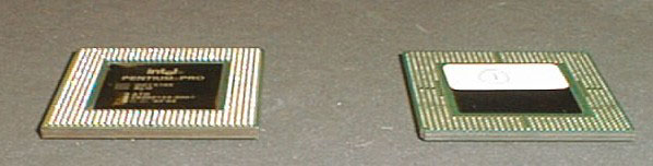
Pentium Pro Package (CPU is left most die along side two 512K cache dies in
the center and right side position). This is a PGA (Pin Grid Array)
type package.
top
Dissection of
Packages
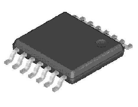 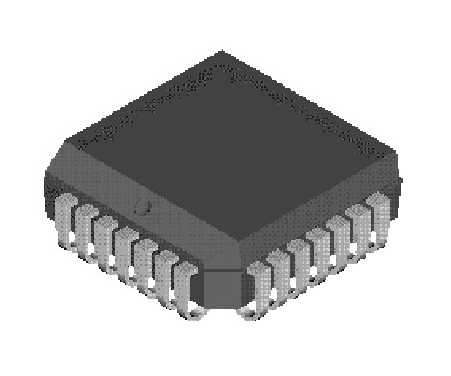
In this lab the students will disect either the SOP (left) (Small Outline Package) or the PLCC (Plastic
Leaded Chip Carrier) (right) and a
Pentium II as shown previously.
top
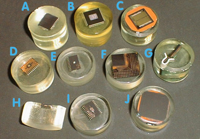
For polishing purposes, portions of each type of package are mounted in
epoxy. The samples are then polished using abrasive papers and silica
polishing wheels in Mueller Hall.
The Samples shown above ahve been polished and are the following views:
A. PLCC wire bonds.
B. PQFP (Plastic Quad
Flat Pack) Die (not dissected this year).
C. Pentium II die.
D. SOP lead frame.
E. SOP die.
F. Pentium II
Lead Frame.
G. Pentium II cross
section.
H. SOP cross section.
I. SOP die
paddle.
J. Pentium
II wire bonds.
top
Micrographs
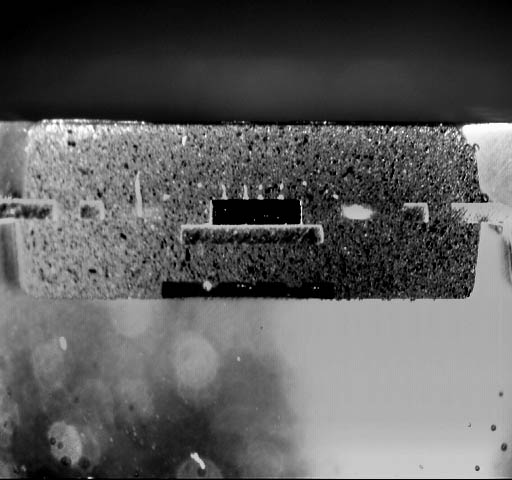
SOP Cross Section (Includes wire bonds on die surface.)
top
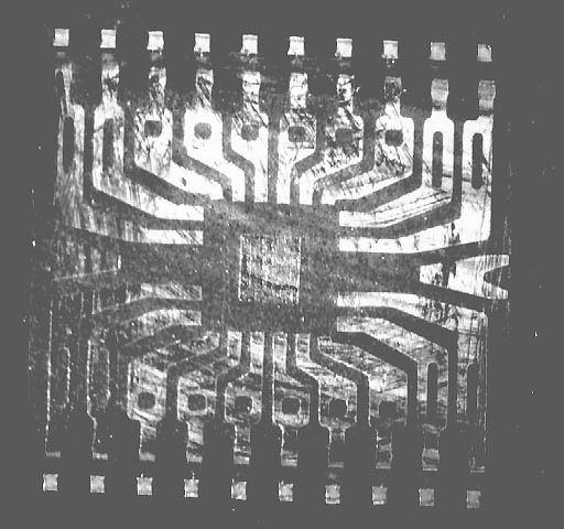
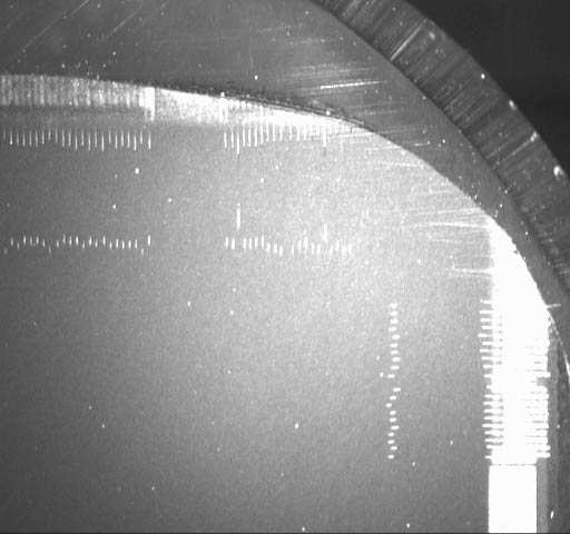
SOP Lead Frame
top
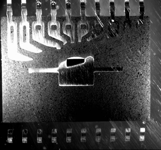
SOP Lead Frame (Showing Die Paddle)
top
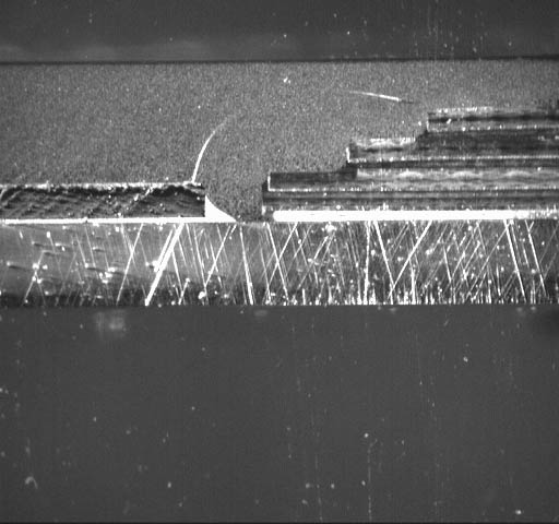
SOP wire bonds
top
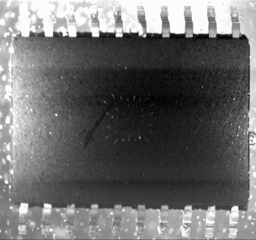
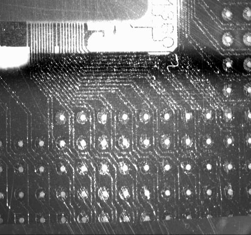
SOP Die
top
Pentium Cross Section (Note: wire bond from die to lead frame.)
top
Pentium Lead Frame
top
Pentium Wire Bonds
top
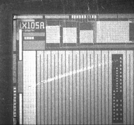
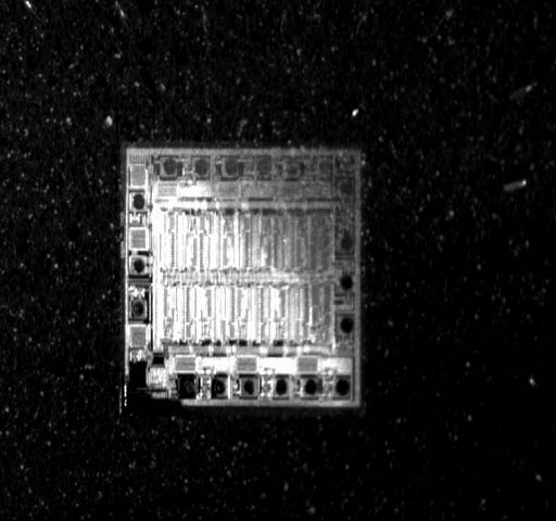
Pentium Die
|