The Hall Effect in Metals and Semiconductors


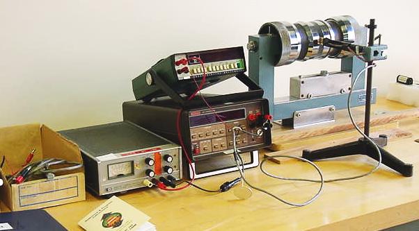
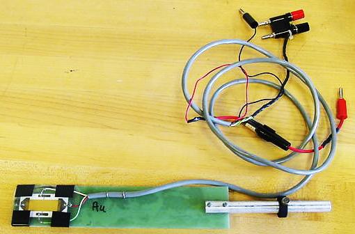
In this experiment, students learn about the classical Hall effect which is the basis of most sensors used in magnetic field measurements. Thin film samples consisting of a semiconductor (InAs) and two different metals (aluminum and gold) are investigated to determine the sign and density of the charge carriers. The sample is placed in a DC magnetic field, and the transverse (Hall) voltage is measured as a function of the current through the sample. Students observe the inverse relationship between the magnitude of the Hall voltage and charge carrier density, a relationship which accounts for the almost exclusive use of semiconductors as Hall effect/magnetic field sensing devices.
Experiment Information
- Lecture slides on Optical Properties of solids (Olmstead) Gives basic theory behind dielectric constants and conductivity.
- Write-up
- Bell 9500 Gaussmeter specifications and operation information.
- Information on the Variflux magnet
Discussion Questions
- Find some values for mobility in tables that are listed in texts, such as Kittel's or other references, such as the Landolt-Bornstein series of books available in the library. Compare your results with the tabulated values. How close are your results to the ones cited for InAs? Can you explain any differences?
- In the case of the aluminum sample, you will find in such texts as Kittel's "Introduction to Solid State Physics" that the assumed charge carriers are "1-hole per atom". Why should we assume that the charge carrier in aluminum is a hole? This is not predicted by the simple Drude theory of electrons in metals.
- Your results for aluminum are likely to be different from the predicted or tabulated values, which are usually quoted as being measured at low temperature and high magnetic field. See what you can find out about the Hall coefficient for a range of temperatures and field strengths, and discuss how your measurement fits in with these.